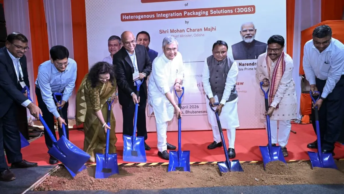
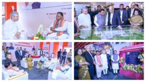
Bhubaneswar: In a significant milestone for India’s semiconductor ambitions, Odisha Chief Minister Mohan Majhi on Sunday laid the foundation stone for 3D Glass Solutions Inc. (3DGS)’s advanced chip packaging facility at Info Valley in Bhubaneswar.
The event was attended by Union Electronics and IT Minister Ashwini Vaishnaw and state’s Electronics and IT Minister Mukesh Mahaling.
Speaking at the event, Vaishnaw praised CM Majhi’s strong commitment to industrial growth and job creation, stating that a “new era of development” has begun in Odisha. He described the glass substrate packaging technology as the future of the semiconductor sector and noted that products from this unit will be the first of their kind manufactured in the country.
Chief Minister Majhi termed the occasion a historic moment not just for Odisha but for India’s technological leadership journey. He pointed to growing global confidence in Odisha, noting interest from leading international firms such as Intel, Lockheed Martin, and Applied Materials. “Odisha has today become the first choice for investors,” he said, citing the state’s abundant natural resources, world-class infrastructure, skilled youth, strong connectivity, and responsive governance as key advantages.
He added that more than Rs 10,000 crore has already been committed to semiconductor projects in Odisha, with companies like RIR Power Electronics and SiCSEM already setting up units.
Majhi envisioned Odisha playing a leading role in Prime Minist
er Narendra Modi’s Atmanirbhar Bharat initiative, positioning the state as the “launchpad” for self-reliant India in eastern India. “If you want to build a career in technology, Odisha is your destination,” he added addressing the youth.
Chief Secretary Anu Garg, and senior officials from both central and state governments, along with 3D Glass Solution President and CEO Babu Mandava were present.

India’s first advanced 3D glass semiconductor packaging unit
The project represents India’s first advanced 3D glass semiconductor packaging unit, establishing Odisha as the first state to host both a compound semiconductor fabrication facility and a cutting-edge 3D chip packaging plant based on glass substrates. The vertically integrated unit will focus on heterogeneous integration packaging solutions, bringing “the world’s most advanced packaging technology” to India.
The facility, with an estimated investment of around Rs 1,943 crore, will use “advanced glass substrate technology to package semiconductor chips required for applications such as artificial intelligence, 5G networks, defence systems and data centres”. Planned annual capacity includes approximately 69,600 glass panel substrates, 50 million assembled units, and 13,200 3DHI modules. It will create more than 2,500 direct and indirect employment opportunities
The project is expected to strengthen domestic semiconductor capabilities and reduce dependence on imports.
The development followed the Union Cabinet’s approval in 2025 for semiconductor projects in Odisha, including this 3DGS initiative with an investment of around Rs 1,943 crore and SiCSem Private Limited’s compound semiconductor fab in collaboration with UK-based Clas-SiC Wafer Fab Ltd. SiCSem’s unit, which broke ground earlier, which aims to produce India’s first commercial silicon carbide (SiC) devices for power electronics in electric vehicles, renewables, and smart grids.