Bhubaneswar: The Biju Janata Dal (BJD) on Sunday slammed the groundbreaking ceremony for India’s first advanced 3D glass semiconductor packaging unit at Infovalley in Bhubaneswar, as a staged publicity stunt rather than a genuine step toward industrial development.
In a press statement, BJD spokesperson Lenin Mohanty accused the BJP of attempting to mislead the people of Odisha by manufacturing a false narrative of industrial progress, even as the state’s investment climate continues to worsen rapidly.
Mohanty pointed out that while the Centre had announced multiple semiconductor projects for Odisha, several key initiatives, including the S Ram and N Ram Semiconductor projects, have already exited the state since the BJP assumed power. Many other major investment proposals have similarly withdrawn, he added.
The BJD leader emphasised that “mere ribbon-cutting and photo-ops do not constitute grounding of investment”. True investment grounding, he said, occurs only when projects actually begin production or start delivering services.
He questioned the current status of numerous similar ribbon-cutting ceremonies conducted by the BJP government last year and asked why the public has not been updated on their progress.
Highlighting the contrast with its own tenure, the BJD claimed that under its rule, Odisha achieved over 34% grounding of investment proposals, significantly higher than the national ‘Make in India’ average of 22%. The party also cited official figures show
ing that Odisha attracted just Rs 39 crore in Foreign Direct Investment (FDI) during 2024-25, among the lowest figures for any major state in the country. It also dismissed the BJP’s claims of “lakh-crore investments” as empty announcements and “blatant propaganda.”
“Empty announcements and photo-shoots cannot substitute for real industrial growth, employment generation, and economic development,” Mohanty stated.
The BJD vowed to continue exposing what it called the “double-engine deception” and to push for genuine, result-oriented investments that deliver tangible benefits to the people of Odisha.
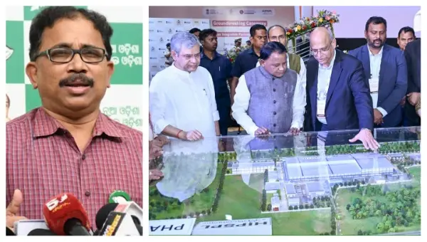
Earlier in the day, Chief Minister Mohan Charan Majhi initiated the groundwork for the chip packaging facility of 3D Glass Solutions Inc. (3DGS), which is expected to introduce high-end manufacturing capabilities to the state. The facility will focus on advanced chip packaging and embedded glass substrate technology to support sectors including artificial intelligence, photonics and high-performance computing.
Also Read: Foundation Laid For India’s 1st Advanced 3D Chip Packaging Unit In Bhubaneswar
This project is one of two semiconductor-related investments cleared earlier by the Centre for Odisha in 2025. The other, led by SiCSem Private Limited, will manufacture silicon carbide-based devices with applications across defence, electric mobility, rail infrastructure and renewable energy systems. Together, these initiatives are part of a wider national effort to expand domestic semiconductor capabilities.
Besides Union Electronics and IT Minister Ashwini Vaishnaw and state’s Electronics and IT Minister Mukesh Mahaling and 3D Glass Solution President and CEO Babu Mandava, Intel CEO Lip-Bu Tan joined the ground breaking on virtual platform.