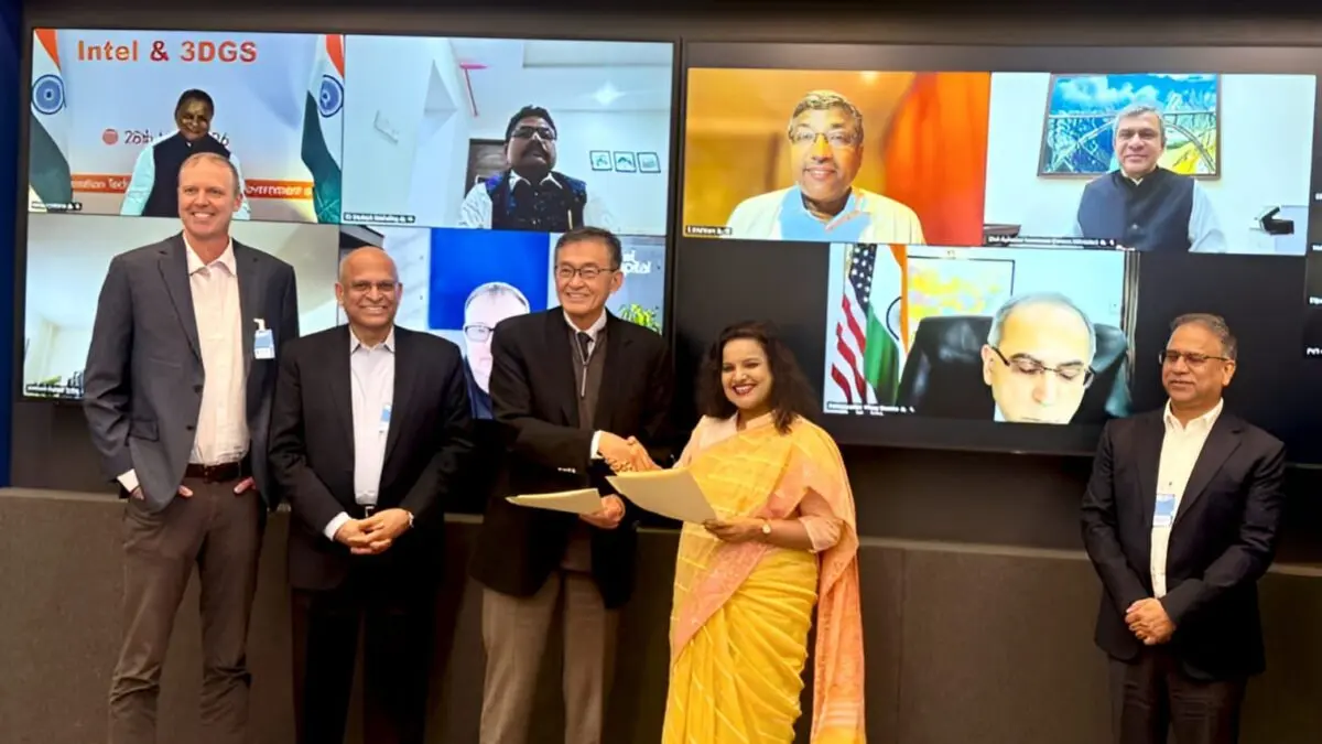
Bhubaneswar/New Delhi: In a significant boost to India’s semiconductor ambitions, the Odisha government has signed a Memorandum of Understanding (MoU) with global chip giant Intel and US-based 3D Glass Solutions (3DGS) to introduce advanced substrate manufacturing technology in the country, Union Minister for Electronics and Information Technology Ashwini Vaishnaw announced on Friday.
“Congratulations to the Govt of Odisha, Intel and 3DGS on signing an MoU to bring substrate manufacturing technology to India. This will further advance semiconductor ecosystem in India,” Vaishnaw posted on X.
The proposed project, to be established in the Bhubaneswar-Khurda region, involves an estimated investment of approximately $3.3 billion, making it one of India’s largest high-technology manufacturing commitments. The facility will specialize in the production of advanced packaging glass core substrates, high-density interconnect substrates, and related semiconductor components, with Intel providing critical technology expertise and process support, the ET reported.
The project is planned for phased implementation over five to six years. Once operational, it is expected to create more than 1,800 direct high-skilled jobs, while also generating significant indirect employment across the electronics manufacturing and semiconductor supply chain ecosystem. State government officials stated tha
t the project will position Odisha as a leading destination for semiconductor and electronics investments, backed by strong infrastructure development and attractive policy incentives aimed at drawing high-technology industries to the state, it added.
The pact builds on Odisha’s growing role in India’s semiconductor landscape. In April 2026, the state laid the foundation stone for the country’s first advanced 3D chip packaging unit at Info Valley in Bhubaneswar. Promoted by 3DGS through its Indian arm, Heterogeneous Integration Packaging Solutions, the project involves an investment of approximately ₹1,943 crore. Once operational, the facility is expected to produce around 69,600 glass panel substrates annually, along with 50 million assembled units and 13,200 advanced 3D heterogeneous integration (3DHI) modules. It will introduce cutting-edge glass substrate and 3D heterogeneous integration technologies critical for high-performance computing, AI, 5G/6G, defence, aerospace, and data centres.
At the April groundbreaking, Minister Vaishnaw described the project as a “historic day” and highlighted Odisha’s emergence as a key IT and semiconductor hub under Prime Minister Narendra Modi’s leadership. Chief Minister Mohan Charan Majhi noted that Odisha is the only state in India hosting both the country’s first compound semiconductor fabrication unit and the first 3D glass substrate packaging facility.
3DGS, a pioneer in advanced glass-based packaging, counts investors including Intel Capital and Lockheed Martin among its backers. The Odisha unit will bring vertically integrated advanced packaging capabilities previously reliant on imports.
This development aligns with the Centre’s push under the Semicon India Programme (India Semiconductor Mission). The government has approved multiple fab and packaging projects nationwide, with recent additions further strengthening the ecosystem. An online Investor Support portal has also been launched to facilitate investments and address industry needs.