New Delhi: In a major boost to India’s chip-making ambitions, the Union Cabinet on Wednesday approved the sixth semiconductor manufacturing unit near the upcoming Noida International Airport at Jewar, under the India Semiconductor Mission.
The project will be a joint venture between India’s HCL Group and Taiwanese electronics giant Foxconn.
“The Union Cabinet has approved India’s 6th semiconductor unit in Jewar, Uttar Pradesh. Under India Semiconductor Mission, 5 semiconductor units have been approved so far and rapid construction is going on there. Production at one unit will begin this year. In this connection, there is one more super-advanced unit. This is a joint venture of HCL and Foxconn…” IT Minister Ashwini Vaishnaw said, briefing the media about the Cabinet meeting chaired by Prime Minister Narendra Modi.
The project involves an investment of Rs 3,700 crore. The facility will have a capacity of 20,000 wafers per month and produce 36 million display driver chips monthly for use in mobile phones, laptops, automobiles, personal computers, and other devices, he further stated.
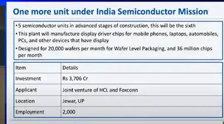
It is expected to generate employment for 2,000 people, he added.
The production of the Jewar unit in Yamuna Expressway Industrial Development Authority or YEIDA is likely to begin in 2027.


